INTRODUCTION:
It is an Analog and mixed signal and the Full Custom IC design tool ,
Revision 1.0 IC613 Assura 32 Incisive Unified Simulator 82
Cadence is an Electronic Design Automation (EDA) environment which allows different applications and tools to integrate into a single framework thus allowing to support all the stages of IC design and verification from a single environment. These
tools are completely general, supporting different fabrication technologies.
Operating System LINUX with minimum 4-GB RAM
OBJECTIVE :
Objective of this lab is to learn the Virtuoso tool as well learn the flow of the Full Custom IC design cycle. You will finish the lab by running DRC, LVS and Parasitic Extraction on the various designs. In the process you will create various components like inverter, NAND or NOR gates Differential amplifier, operational amplifier, R-2R based DAC and Mixed signal design of SAR based ADC, but we won’t be designing every cell, as the time will not be sufficient, instead we will be using some ready made cells in the process.
WORKING PRINCIPLE :
You will start this lab by creating a library called “myDesignLib(Or any other you want )” and you will attach the library to a technology library for example “gpdk180”. Attaching a technology library will ensure that you can do front to back design. After this you will create a new cell called “Inverter or which circuit you want to design” with schematic view and hence build the Inverter schematic by instantiating various components. Once inverter schematic is done, symbol for “Inverter” is generated. Now you will create a new cell view called “Inverter_Test”, where you will instantiate “Inverter” symbol. This circuit is verified by doing various simulations using spectre. In the process, you will learn to use spectre, waveform window options, waveform calculator, etc... You will learn the Layout Editor basics by concentrating on designing an “Inverter” through automatic layout generation . Then you will go ahead with completing the other layouts. After that, you will run DRC, LVS checks on the layout, Extract parasitics and back-annotate them to the simulation environment.
How to Start
The software will be install in the root plate form
Open Terminal
Type "cd cadence" (press Enter)
"csh" (press Enter)
"source cshrc" (press Enter)
After pressing enter a message "welcome to cadence tools" will be display
"cd Database" (press Enter)
"cd cadence" (and press tab) cd cadence _analog_Labs_613 will display then press Enter and at last type
"virtuoso" (press Enter)
this is also shown by figure below

When you press enter after command "virtuoso" A CDS. log window ( it also called Main window ) will open as given below

Example INVERTER:Now we take an example of Inverter for more knowledge about this tool
here new Library name is "Usmani" and new Cell name is "Inverter"
1) Create own Library and Cell
2) Schematic Entry .
3) Symbol Creation
4) Building the Inverter_Test Design
5) Analog Simulation with Spectre
6) Parametric Analysis
7) Creating Layout View of Inverter
8) Physical Verification
In the CDS.log window or Main window goto "File >New >Library" as show given figure

When you click on Library a new window will open for creating new Library name, I already mentioned you, new library name is "Usmani" so you will write "Usmani" in the Library name column, and this library will attach to an existing technology library also shown by figure

after creating new library name "Usmani" and it attached by existing library click on "OK" a new window will open like below, here you will choose any one existing technology library suppose here we choose "gpdk180" then click "OK"

How to Start
Open Terminal
Type "cd cadence" (press Enter)
"csh" (press Enter)
"source cshrc" (press Enter)
After pressing enter a message "welcome to cadence tools" will be display
"cd Database" (press Enter)
"cd cadence" (and press tab) cd cadence _analog_Labs_613 will display then press Enter and at last type
"virtuoso" (press Enter)
this is also shown by figure below

When you press enter after command "virtuoso" A CDS. log window ( it also called Main window ) will open as given below

Example INVERTER:Now we take an example of Inverter for more knowledge about this tool
here new Library name is "Usmani" and new Cell name is "Inverter"
Building Blocks of an Inverter:
1) Create own Library and Cell
2) Schematic Entry .
3) Symbol Creation
4) Building the Inverter_Test Design
5) Analog Simulation with Spectre
6) Parametric Analysis
7) Creating Layout View of Inverter
8) Physical Verification
9) Creating the Configuration View
10) Generating Stream Data
10) Generating Stream Data
1) Create own Library and Cell
In the CDS.log window or Main window goto "File >New >Library" as show given figure

When you click on Library a new window will open for creating new Library name, I already mentioned you, new library name is "Usmani" so you will write "Usmani" in the Library name column, and this library will attach to an existing technology library also shown by figure

after creating new library name "Usmani" and it attached by existing library click on "OK" a new window will open like below, here you will choose any one existing technology library suppose here we choose "gpdk180" then click "OK"

After clicking on "OK", in the CDS.log window or Main window a new message "Successfully attached to an existing technology library gpdk180 " will display
Now you have to create new "Cellview" , so go to the CDS.log window or Main window and then go to the File>New>Cellvie, such as

Now you have to create new "Cellview" , so go to the CDS.log window or Main window and then go to the File>New>Cellvie, such as

a new window will open set it as
library .............Usmani
Cell ..................Inverter"
View ................Schematic
Open with........Schematic L
this is also shown by below figure

when you will click "Ok" a new blank black window will open such as
Note: its Optional
You can also check your library name and cellview in the library list in the CDS.log window or Main window go to the "Tools" and click on "Library Manager" a new window will open

Here you can check your "Library" name and "Cell" name
An Inverter Schematic Capture

This is an Inverter schematic diagram now we have to create similarly an Inveter by cadence Virtuoso tool in a black blank window
2) SCHEMATIC ENTRY
 |
| Adding component fixed menu icon
Note: Use of any kind of power source like Voltage source or Current source
are not allowed in Schematic and Layout operation you can use only pin in place of that,
but in Test operation you can use directly this sources. |
 Adding Components to schematic
 1. In the Black blank Inverter schematic window, click the Instance fixed menu icon
to display the Add Instance form.
Tip: You can also execute Create > Instance or press i. a new window is pop up

2. Click on the Browse button, This opens up a Library browser from which you can select components and the symbol view . In this window there are three category column I) Library II) Cell and III) View now you have to choose gpdk180 in the Library column, pmos in Cell column and symbol in View column and this is also shown by figure below

as clicking on symbol a new window will open, as below

now you will update the parameters in this new window as given in the table
Library name Cell Name Parameters
gpdk180 pmos For M0: Model name = pmos1, Total Width= wp, Length=180n
(Note: Please change the value of width "wp" in place of 2u and Finger width automatically will change, only in PMOS case not NMOS)
(Note: Please change the value of width "wp" in place of 2u and Finger width automatically will change, only in PMOS case not NMOS)
gpdk180 nmos For NM0: Model name =nmos1, total width= 2u, Length =180n
3) Process 1 and 2 will do as it is for nmos selection and its parameters are already given above in the table
| fixed menu Icon for correction |
III) You can also rotate components at the time you place them, by just press "r" (for component rotation ) and "ctrl+ r" (for arrow rotation) or use the Edit— Rotate command after they are placed.
4. After entering components, press "Esc" with your cursor in the schematic window.
 Adding pins to Schematic
1. Click the Pin fixed menu icon in the schematic window. You can also execute Create > Pin or press "p".the Add pin form appears. as given below

2. Type the following in the Add pin form in the exact order leaving space
between the pin names.
Pin Names Direction
vin Input
vout Output
Make sure that the direction field is set to input/output/inputOutput when placing the input/output/inout pins respectively and the Usage field is set to schematic.
3. Select "Hide" from the Add – pin form after entering the the pin name.
and the use "Esc" in the schematic window after placing it in right place,
 Adding wire to Schematic
1. Click the Wire (narrow) icon in the schematic window.
You can also press the "w" key, or execute Create > Wire (narrow).
2. In the schematic window, click on a pin of one of your components as the first point for your wiring. A diamond shape appears over the starting point of this wire.
3. Follow the prompts at the bottom of the design window and click left o n the destination point for your wire. A wire is routed between the source and destination points.
4. Complete the wiring as shown in figure and when done wiring press "ESC" key in the schematic window to cancel wiring.
if you want to delete wrong wire connection so firstly select the that wire and use "Delete fixed icon" which is 4th symbol from above icon or go to the "Edit > Delete"
Saving the Design


1. Click the Check and Save icon in the schematic editor window.
2. Observe the CIW output area for any errors.
3) Symbol Creation
In this section, you will create a symbol for your inverter design so you can place it in a test circuit for simulation. A symbol view is extremely important step in the design process. The symbol view must exist for the schematic to be used in a hierarchy. In addition, the symbol has attached properties(cdsParam) that facilitate the simulation and the design of the circuit.
1. In the Inverter schematic window, execute
Create > Cellview > From Cellview.
The Cellview From Cellview form appears. With the Edit Options
function active, you can control the appearance of the symbol to
generate.
2. Verify that the From View Name field is set to schematic, and the Tool View Name field is set to symbol, with the Tool/Data Type set
as SchematicSymbol.


4. Modify the Pin Specifications: You should arrange the Pin name as follows

5. Click OK in the Symbol Generation Options form.
6. A new window displays an automatically created Inverter symbol as shown here.
Editing a Symbol

Note: From point 2 to 6 are Optional
In
this section we will modify the inverter symbol to look like a Inverter gate symbol.
1.Click Delete icon
in the symbol window and Delete the red rectangular box and goto "Create > Selection Box" a new window "Add Selection Box" will pop-up

and then click on "Automatic" again a red rectangular box will appear
2. Similarly Delete the green rectangular box
3. Execute "Create > Shape > Circle" to make a
circle at the end of triangle.
4. After creating the triangle press ESC key.
5. Execute "Create > Shape > polygon", and draw a shape similar to triangle
4. After creating the triangle press ESC key.
5. Execute "Create > Shape > polygon", and draw a shape similar to triangle
6.
You can move the pin names according to the location.
7.
After creating symbol, click on the save icon in the symbol
editor window to save the symbol. In the symbol editor, execute "File > Close" to close the symbol view window.

4) Building the Inverter_Test Design
Open new Inverter_Test window
1. In
the CIW or Library Manager, execute" File > New > Cellview "
2.
Set up Usmani in Library column and Inverter_Test in Cell column the New File form as follows

3.
Click "OK" when done. A blank schematic window for the Inverter_Test
design appears.
Building the Inverter_Test Circuit
1.Click "Adding fixed menu Icon > browse " a Library manager will open now choose library name, cell name and Properties as given below in the table and build the build
the Inverter_Test schematic.
Library
name
|
Cellview
name
|
Properties/Comments
|
Usmani
|
Inverter
|
Symbol
|
analogLib
|
Vpulse
|
v1=0, v2=1.8,td=0 tr=tf=1ns, ton=10n, T=20n
|
analogLib
|
vdc, gnd
|
vdc=1.8
|
Note: Remember
to set the values for VDD and VSS. Otherwise, your circuit will
have no power.
 2.
Add the above components using "Create > Instance" or by pressing "I". or click on this icon
2.
Add the above components using "Create > Instance" or by pressing "I". or click on this icon
3.
Click the " Wire (narrow)" icon and wire your schematic.
Tip: You
can also press the w key, or execute" Create > Wire (narrow)."
4. Click "Create > Wire Name" or press "L" to name the input (Vin) and output (Vout) wires as in the below schematic.
5. Click on the "Check and Save" icon to save the design.
5. Click on the "Check and Save" icon to save the design.
6.
The schematic should look like this.

7.
Leave your Inverter_Test schematic window open for the next
section.

To view the model file, highlight the expression in the Model Library File field and Click Edit File.
2. To complete the Model Library Setup, move the cursor and click "OK".
 Running the Simulation

6) Parametric Analysis

 Note: Change the wp value
of pmos device back to 2u and save the schematic before proceeding to the next
section of the lab. To do this use edit property option.
Note: Change the wp value
of pmos device back to 2u and save the schematic before proceeding to the next
section of the lab. To do this use edit property option.
Step 1: PMOS enclose with n-well
Goto LSW Window and select Nwell and then goto Create > Shape >Rectangle and draw a rectangle(only PMOS enclose in it)
Step 2: Goto Create > Via a new window will pop-up and select M1_NWELL a rectagular box will appear and put this box in rectagular NWell box and above the PMOS
Step 3: Put Vdd pin (See only after 4 to 5 times zooming window) on or left or right side of the M1_NWELL box
Step 4: Goto LSW window and select Metal1 and press P or goto Create> Shape > Path and create the connection as shown in given figure


8) Physical
Verification
(Assura DRC)


3. In the Extraction tab of
the form, choose Extraction type, Cap Coupling Mode and specify the Reference
node for extraction.


4. Click "Use template" at the bottom of the New Configuration form and

select Spectre in the cyclic field and click "OK".


7. Click the Tree View tab.
The design hierarchy changes to tree format. The form should look like this:


 5.
Click "Netlist and Run" icon to start
the simulation.
5.
Click "Netlist and Run" icon to start
the simulation.

1. In the waveform window execute Tools > Calculator.

 7.
Click on "Evaluate the buffer
icon"
7.
Click on "Evaluate the buffer
icon"
 4.
Click on the Recompute the hierarchy
icon,
4.
Click on the Recompute the hierarchy
icon,
the configuration is
now updated from schematic to av_extracted view.
6.
From the Analog Design Environment
window click Netlist
and Run to
 3. In
the StreamOut-Options form
select
3. In
the StreamOut-Options form
select
under Layers tab and click" OK".
 3. In
the StreamOut-Options form
select
3. In
the StreamOut-Options form
select
under Layers tab and click "OK".
5) Analog Simulation with Spectre
Objective: To set up and run
simulations on the Inverter_Test design
In
this section, we will run the simulation for Inverter and plot the transient,
DC characteristics and we will do Parametric Analysis after the initial
simulation.
Starting the Simulation Environment
Start
the Simulation Environment to run a simulation.
1. In
the Inverter_Test schematic window,
execute "Launch > ADE L"
The Virtuoso Analog Design Environment (ADE)
simulation window appears given below

 1. In
the Simulation window,go to Variables > Edit .
1. In
the Simulation window,go to Variables > Edit .
3. Set the value of the "wp" variable by Click on "wp" (which is right hand side of the window)
3. Click "OK" or Cancel in the Editing Design Variables window.
Setting Design
Variables
Set
the values of Total Width of PMOS in the circuit before simulating. Otherwise,
the simulation will not run.
The
Editing Design Variables form appears as given below.
2. Click "Copy From" at the bottom of the form.
2. Click "Copy From" at the bottom of the form.
The
design is scanned and all variables found in the design are listed.
In a
few moments, the wp variable
appears in the Table of Design variables section as given below

3. Set the value of the "wp" variable by Click on "wp" (which is right hand side of the window)
and enter
the following:
Value(Expr)
|
2u
|
Click on "Change" and notice the update in the Table of Design Variables as given below

3. Click "OK" or Cancel in the Editing Design Variables window.
Choosing a Simulator
Set
the environment to use the Spectre® tool,
a high speed, highly accurate
analog
simulator. Use this simulator with the Inverter_Test
design, which is made-up of analog components.
1. In
the simulation window (ADE), execute
"Setup > Simulator/Directory/Host".
2. In
the Choosing Simulator form, set the Simulator field to spectre (Not
spectreS) & click "OK"
Setting the Model Libraries
The
Model Library file contains the model files that describe the nmos and pmos devices
during
simulation.
1. In the simulation window (ADE),
Execute
Setup > Model Libraries.
The
Model Library Setup form appears. Click the browse button to add gpdk.scs if not added by default as
shown in the Model Library Setup
form.
Remember
to select the section type as stat
in front of the gpdk.scs file.
Your
Model Library Setup window should now looks like the below figure.


To view the model file, highlight the expression in the Model Library File field and Click Edit File.
2. To complete the Model Library Setup, move the cursor and click "OK".
The
Model Library Setup allows you to include multiple model files.
It
also allows you to use the Edit button to view the model file.
Choosing Analyses
This
section demonstrates how to view and select the different types of analyses to complete
the circuit when running the simulation.
1. In
the Simulation window (ADE L), click the Choose > Analyses icon.
You
can also execute Analyses > Choose.
The
Choosing Analysis form appears. This is a dynamic form, the bottom of the form
changes
based on the selection above.
2. To
setup for transient analysis
a. In the Analysis section select "tran"
b. Set the stop time as 200n
c. Click at the moderate or Enabled button
at the bottom, and then click "Apply".


3. To
set up for DC Analyses:
a. In the Analyses section, select "dc".
b. In the DC Analyses section, turn on Save DC Operating Point.
c. Turn on the Component Parameter.
d. Double click the Select Component, after double click cursor will goes to Test schematic
d. Double click the Select Component, after double click cursor will goes to Test schematic
e. Click input signal vpulse source in the test schematic
window.
a new window will popup
a new window will popup
f. Click “DC Voltage” in the Select
Component Parameter form and click OK.
f. In the analysis form type start and stop voltages as 0 to
1.8 respectively.
g. Check the enable button and then
click Apply.


4.
Click "OK" in the Choosing Analyses Form.
Selecting Outputs for Plotting
1.
Execute "Outputs > To be plotted > Select on Schematic" in the simulation window.
2.
Follow the prompt at the bottom of the schematic window, Click on output
net Vout, input net Vin of the Inverter. Press ESC with the cursor in the schematic after selecting
it.
Does the simulation window look like this?


1.
Execute Simulation > Netlist and
Run in the simulation window to start the
Simulation
or the icon, this will create the netlist as well as run the simulation.
2.
When simulation finishes, the Transient, DC plots automatically will be popped
up along with log file.

Saving the Simulator
State
We
can save the simulator state, which stores information such as model library
file,
outputs,
analysis, variable etc. This information restores the simulation environment
without
having to type in all of setting again.
1. In
the Simulation window, execute Session > Save State.
The
Saving State form appears.
2.
Set the Save as field
to state1_inv and make
sure all options are selected under
what
to save field.
3.
Click "OK" in the
saving state form. The Simulator state is saved.
Loading the Simulator State
1.
From the ADE window execute Session > Load State.
2. In
the Loading State window, set the State name to state1_inv as shown


3.
Click "OK" in the Loading State
6) Parametric Analysis
Parametric
Analysis yields information similar to that provided by the
Spectre® sweep feature, except the data is for a full
range of sweeps for each
parametric
step. The Spectre sweep feature provides sweep data at only one
specified
condition.
You
will run a parametric DC analysis on the wp
variable, of the PMOS device of the Inverter design
by sweeping the value of wp.
Run a
simulation before starting the parametric tool. You will start by loading the
state from the previous simulation run.
Run
the simulation and check for errors. When the simulation ends, a single
waveform in the waveform window displays the DC Response at the Vout node.
Starting the Parametric Analysis Tool
1.
In the Simulation window, execute Tools > Parametric Analysis.
The Parametric Analysis form appears.

2. Double click on "Add variable" and select "wp".
3. Change the Range Type and Step Control fields in the Parametric
2. Double click on "Add variable" and select "wp".
3. Change the Range Type and Step Control fields in the Parametric
Analysis form as shown below:
Variable Range Type From To Step mode Total
Steps
wp From/To 1u 10u Auto 10
These
numbers vary the value of the wp of
the pmos between 1um and 10um at ten
evenly spaced intervals.

5.
Execute Analysis > Start.
The
Parametric Analysis window displays the number of runs remaining
in the analysis and the current value of the swept variable(s). Look in the
upper right corner of the window. Once the runs are completed the wavescan
window comes up with the plots for different runs.

7) Creating Layout View of Inverter
 Layout View

Note: Goto the Schematic window of the Inverter and change the value of the "Total Width" of PMOS from "wp" to any constant value, for example 2u
From the Inverter schematic window menu execute
"Launch – Layout XL". A Startup Option form
appears.
Select
"Create New" option. This gives a New Cell View Form


• Check
the Cellname (Inverter), Viewname (layout). as given below

• Click
"OK" from the
New Cellview form.
• LSW
and a blank layout window appear along with schematic window.
•Execute " Connectivity > Generate > All from Source" in the new
blank black window, Generate Layout form
appears. Click "OK"
which imports the schematic components into the Layout window
automatically. and here in this case one PMOS one NMOS ,four
small rectangle one for Vdd terminal, one for Vss, one for input and
one for output will appear
Q ) How you know about each small rectangle ?
Ans) Firstly put the cursor on any box and click on "Q"
•Execute "Connectivity>Nets>Show/Hide selected IncompleteNets"
•Execute " Connectivity > Generate >Place As In Schematic" a
warning window popup click "Yes" then automatically MOS are
shifted in rectangular boundary
Use "Edit and Adding componet fixed menu icon" for putting the each
component as given layout
Creating Contacts/Vias
Note 1: You will use
the contacts or vias to make
connections between two different layers
Execute "Create > Via" or
select command to place different
Contacts, as given in below table
Connection Contact Type
For
Metal1- Poly Metal1-Poly
For Metal1- Psubstrate Metal1-Psub
For Metal1- Nwell Metal1-Nwell
Note 2: PMOS always enclose with n-well rectangle
For Metal1- Psubstrate Metal1-Psub
For Metal1- Nwell Metal1-Nwell
Note 2: PMOS always enclose with n-well rectangle
Goto LSW Window and select Nwell and then goto Create > Shape >Rectangle and draw a rectangle(only PMOS enclose in it)
Step 2: Goto Create > Via a new window will pop-up and select M1_NWELL a rectagular box will appear and put this box in rectagular NWell box and above the PMOS
Step 3: Put Vdd pin (See only after 4 to 5 times zooming window) on or left or right side of the M1_NWELL box
Step 4: Goto LSW window and select Metal1 and press P or goto Create> Shape > Path and create the connection as shown in given figure

Layout view in part wise 1 of 3
: Connection of Input
1) Goto LSW window and click on Poly and press p, and
connect the NMOS gate by PMOS gate through these poly
2) Goto Create>Via > M1_Poly, a small box will appear, put
this box inbetween of this MOS and put the Input terminal
on M1_poly box
3) and make the connection in between connection line of
these two MOS and input terminal through poly line, this
is also shown by figure below

Layout view in part wise 2 of 3
Note 3: Connection of Vss
1)Goto Create>Via > M1_ psub, a box will appear put this box
below the NMOS and also put Vss terminal on this box
2) Goto LSW window and click on Mettle 1 and press p and
make the connection as given below

Layout view in part wise 3 of 3
Saving the design
Save your design by selecting "File > Save"
8) Physical
Verification
(Assura DRC)
Running a DRC
1.
Open the Inverter layout form the CIW or
library manger if you have closed that. Press
"shift > f" in the layout window to display all the levels.
library manger if you have closed that. Press
"shift > f" in the layout window to display all the levels.
2.
Select "Assura > Run DRC " from
layout window.
The
DRC form appears. The Library and Cellname
are taken from the current design window, but
rule file may be missing. Select the Technology
as gpdk180. This automatically loads the rule file.
are taken from the current design window, but
rule file may be missing. Select the Technology
as gpdk180. This automatically loads the rule file.
Your
DRC form should appear like this

3.
Click "OK" to start
DRC.
4. A
Progress form will appears. You can click on the watch log file to see the log file.
5.
When DRC finishes, a dialog box appears asking you if you want to view your DRC
results, and then click "Yes" to view the results
of this run.
6. If
there any DRC error exists in the design View
Layer Window (VLW) and Error
7.
Click View > Summary in
the ELW to find the details of errors.
8.
You can refer to rule file also for more information, correct all the DRC
errors and "Re > run" the DRC.
9. If
there are no errors in the layout then a dialog box appears with No DRC errors
ASSURA
LVS
In
this section we will perform the LVS check that will compare the schematic
netlist and
the
layout netlist.
Running LVS
1.
Select "Assura – Run LVS" from the
layout window.
The
Assura Run LVS form appears. It will automatically load both the schematic and
layout view of the cell.
2.
Change the following in the form and click "OK".

3.
The LVS begins and a Progress form appears.
4. If
the schematic and layout matches completely, you will get the form displaying Schematic and Layout Match.
5. If
the schematic and layout do not matches, a form informs that the LVS completed successfully
and asks if you want to see the results of this run.
6.
Click "Yes" in the
form.
LVS
debug form appears, and you are directed into LVS debug environment.
7. In
the LVS debug form you can find the
details of mismatches and you need to
Assura RCX
In
this section we will extract the RC values from the layout and perform analog
circuit simulation
on the designs extracted with RCX.
Before
using RCX to extract parasitic devices for simulation, the layout should
match
with schematic completely to ensure that all parasites will be back an noted to
the correct
schematic nets.
Running RCX
1.
From the layout window execute "Assura > Run RCX".
2.
Change the following in the Assura parasitic extraction form. Select output type under Setup tab of the form.
|

|

|

4. In
the Filtering tab of the form, Enter Power Nets as vdd!, vss! and Enter Ground Nets as gnd!

5. Click "OK" in the Assura parasitic extraction form when done.
The
RCX progress form appears, in the progress form click Watch log file to see the
output log file.
5.
When RCX completes, a dialog box appears, informs you that Assura RCX run
Now minimized the all window and except CDS.log or main window
go to " File > Open , a new window will popup, now set av_extracted in the view column such as
Now minimize the all window and open CDS.log or main window and
goto " File > open " a new window will open , now set this window
Selected Input Enable Function Type
Vin just click Pulse Voltage
Choosing Analysis
execute "Analyses > Choose".
Running the Simulation
Now minimized the all window and except CDS.log or main window
go to " File > Open , a new window will popup, now set av_extracted in the view column such as
Starting the Simulation Environment
Now minimize the all window and open CDS.log or main window and
goto " File > open " a new window will open , now set this window
as Library name as Usmani, cell name as Inverter , view as av_extracted and Type as layout
a inverter av_extracted black window will open goto "Launch > ADE L" a observation table will open goto " setup > stimuli..." a new window will popup here we will enter parameters of inputs as below
a inverter av_extracted black window will open goto "Launch > ADE L" a observation table will open goto " setup > stimuli..." a new window will popup here we will enter parameters of inputs as below
Selected Input Enable Function Type
Vin just click Pulse Voltage
a new parameter window will
pop up, now fill the value as given previous in the table of Test
schematic operation and click on "apply" similarly you will fill the value of Vdd=1.8v and Vss =0v and click "Ok"
now goto Observation table
Choosing Analysis
execute "Analyses > Choose".
The
Choosing Analysis form appears. This is a dynamic form, the bottom of the form
changes
based on the selection above.
Here we only perform Transient Analysis
To
setup for transient analysis
a. In the Analysis section select "tran"
b. Set the stop time as 200n
c. Click at the moderate or Enabled button
at the bottom, and then click "Apply".
Selecting Outputs for Plotting
1.
Execute "Outputs > To be plotted –
Select on Schematic" in the simulation window.
2.
Follow the prompt at the bottom of the schematic window, Click on output
net Vout, input net Vin of the Inverter. Press ESC with the cursor in the schematic after selecting
it.Running the Simulation
1.
Execute Simulation > Netlist and
Run in the simulation window to start the
Simulation
or the icon, this will create the netlist as well as run the simulation.
2.
When simulation finishes, the Transient, DC plots automatically will be popped
up along with log file.
In
this section we will create a config view and with this config view we will run
the simulation
with and without parasitic.
1. In
the CIW or Library Manager, execute "File > New > Cellview"
2. In
the Create New file form, set the following:
Usmani in Library, Inverter_Test in Cell column and Config in view column

Usmani in Library, Inverter_Test in Cell column and Config in view column

3.
Click "OK"
The Hierarchy Editor form opens and a New Configuration form opens in front
of it.
 |
|

4. Click "Use template" at the bottom of the New Configuration form and
The
Global Bindings lists are loaded from the template.

select Spectre in the cyclic field and click "OK".
a new window will popup

5.
Change the Top Cell View to schematic
and delete the default entry from the
6.
Click "OK" in the
New Configuration form.
The
hierarchy editor window will open and it displays the hierarchy for this design using table format.


8. Save
the current configuration.
9.
Close the Hierarchy Editor window. Execute "File > Close Window".
To run the Circuit without Parasites
1.
From the Library Manager open Inverter_Test
Config view.
Open
Configuration or Top cellview form appears.

2. In
the form, turn on the both cyclic buttons to "Yes" and click "OK".
The
Inverter_Test schematic and Inverter_Test config window appears. Notice the
windowbanner of schematic also states Config: Usmani Inverter_Test config.
3.
Execute "Launch > ADE L" from the schematic window.
4.
Now you need to follow the same procedure for running the simulation. Executing
in the ADE L Window go to "Session > Load state", the Analog
Design Environment window loads the previous state.
The
simulation takes a few seconds and then waveform window appears.
6. In
the CIW, note the netlisting statistics in the Circuit inventory section. This list
includes all nets, designed devices, source and loads. There are no
parasitic
components. Also note down the circuit inventory section.
Measuring the Propagation Delay
The
calculator window appears.

2.
From the "special functions" select delay, this will open the delay data panel.
3.
Place the cursor in the text box for Signal1, select the wave button and select the
input waveform from the waveform window.
4.
Repeat the same for Signal2, and select the output waveform.
5.
Set the Threshold value 1 and
Threshold value 2 to
0.9, this directs the
calculator
to calculate delay at 50% i.e. at 0.9 volts.
6.
Execute "OK" and observe
the expression created in the calculator buffer.
8.
Close the calculator window.
To run the Circuit with Parasites
In
this exercise, we will change the configuration to direct simulation of the av_extracted view which contains the
parasites.
1.
Open the same Hierarchy Editor form, which is already set for Inverter_Test
config.
2.
Select the Tree View icon:
this will show the design hierarchy in the tree format.
3.
Click right mouse
on the Inverter schematic.
A
pull down menu appears. Select av_extracted
view from the Set
Instance view menu, the View to use column now shows
av_extracted view.


start
the simulation again.
7.
When simulation completes, note the Circuit
inventory conditions, this time the list shows all nets, designed
devices, sources and parasitic devices as well.
8.
Calculate the delay again and match with the previous one. Now you can conclude
how much delay is introduced by these parasites, now our main aim should to
minimize the delay due to these parasites so number of iteration takes place
for making an optimize layout.
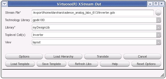
10) Generating Stream Data
Streaming Out the Design
1.
Select "File > Export > Stream" from
the CIW menu and Virtuoso Xstream out
form appears change the following in the form.

2.
Click on the "Options" button.
4. In
the Virtuoso XStream Out form, click
Translate button to
start the stream translator.
5. The stream file Inverter.gds is stored in the
specified location.
Streaming In the Design
1.
Select File – Import – Stream from
the CIW menu and change the following
in
the form.

You
need to specify the gpdk180_oa22.tf file.
This is the entire technology file that
has
been dumped from the design library.
2.
Click on the Options button.
4. In
the Virtuoso XStream Out form, click
Translate button to
start the stream translator.
5.
From the Library Manager open the Inverter
cellview from the GDS_LIB
library
and notice the design.
6. Close all the windows except CIW window, which is
needed for the next lab
hey zoha usmani
ReplyDeleteiam presently pursuing my btech degree from vardhaman college of engineering.. can u please send me list of project details at btech level in cadence virtuoso platform..it would be very helpful for me.. please kindly mail me the project details or list of projects at archith.manne@gmail.com
Awesome Informative post brother............helped alot for me am very grateful!!!!
ReplyDeleteMerci pour la présentation, peut on réaliser un inverseur NMOS chargé par un depletion mos connecté à VGS=0 en utilisant les composants de la librairie gpdk180 v3-3.
ReplyDelete